


404
Oops! Page Not Found
We're sorry, but the page you're looking for doesn't exist or has been moved please browse our other articles.
We're sorry, but the page you're looking for doesn't exist or has been moved please browse our other articles.
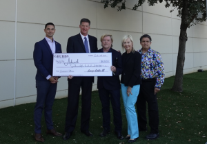
George Grubbs and Seth Levin of Grubbs Family of Dealerships presents Arkearth with grant check Arkearth.org - saving pollinators . planting wildflowers . Arkearth features pollination houses in many of its projects for gardens , farms , and schools Arkearth 's grant from Grubbs Family of Dealerships will provide pollination
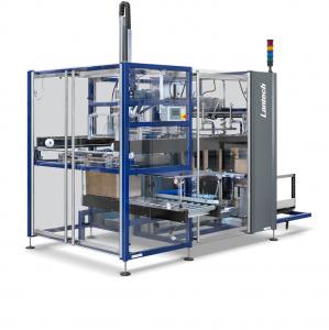
Lantech tray erectors produce trays in a simple , safe operation that eliminates machine jams and downtime costs . Lantech is a global leader in packaging automation equipment . Lantech , a global leader in packaging automation equipment , is proud to announce that its Tray and Lid equipment is
The Mystic Mermaid is a proprietary oyster available only at Fish City Grill and Half Shells locations . Acclaimed seafood destinations will launch proprietary oyster on Nov. 19 The launch of the Mystic Mermaid allows us to create a truly unique experience for our diners. ” — Lovett Bayne ,
John Bayne , a former senior vice president and general manager at Corning , Inc. , brings more than three decades of experience to NS Nanotech at a time when it is readying multiple innovations for commercial markets . A former senior executive at Corning , Inc. , John Bayne
The companies new location will be a major regional hub , able to handle large and small contracts . Nationally recognized company aims to dramatically improve service levels for public safety vehicles and related equipment in the New Mexico region . Our shops are tailor-fit for fast production and the